Chapter 4 contributes to program execution. Understand a simple - PowerPoint PPT Presentation
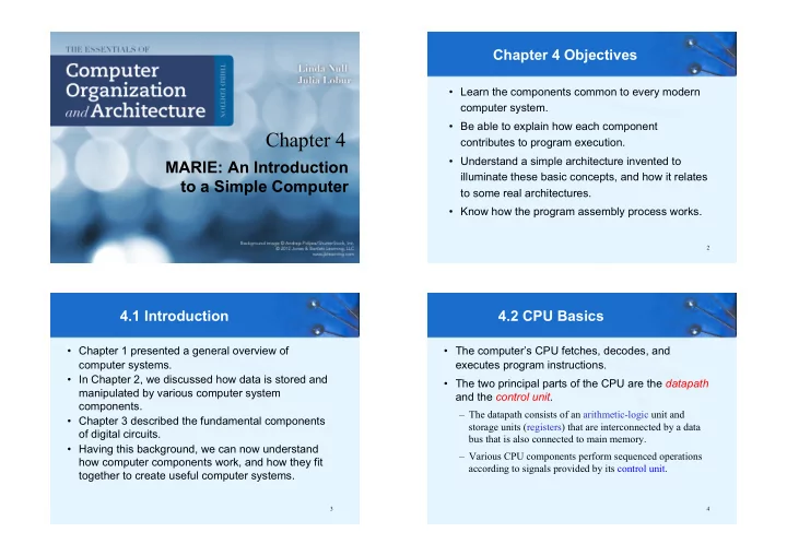
Chapter 4 Objectives Learn the components common to every modern computer system. Be able to explain how each component Chapter 4 contributes to program execution. Understand a simple architecture invented to MARIE: An Introduction
Chapter 4 Objectives • Learn the components common to every modern computer system. • Be able to explain how each component Chapter 4 contributes to program execution. • Understand a simple architecture invented to MARIE: An Introduction illuminate these basic concepts, and how it relates to a Simple Computer to some real architectures. • Know how the program assembly process works. 2 4.1 Introduction 4.2 CPU Basics • Chapter 1 presented a general overview of • The computer’s CPU fetches, decodes, and computer systems . executes program instructions . • In Chapter 2, we discussed how data is stored and • The two principal parts of the CPU are the datapath manipulated by various computer system and the control unit . components. – The datapath consists of an arithmetic-logic unit and • Chapter 3 described the fundamental components storage units (registers) that are interconnected by a data of digital circuits. bus that is also connected to main memory. • Having this background, we can now understand – Various CPU components perform sequenced operations how computer components work, and how they fit according to signals provided by its control unit. together to create useful computer systems. 3 4
4.2 CPU Basics 4.3 The Bus • Registers hold data that can be readily accessed by • The CPU shares data with other system components the CPU. by way of a data bus. – A bus is a set of wires that simultaneously convey a single • They can be implemented using D flip-flops . bit along each line. – A 32-bit register requires 32 D flip-flops. • Two types of buses are commonly found in computer • The arithmetic-logic unit (ALU) carries out logical and systems: point-to-point , and multipoint buses. arithmetic operations as directed by the control unit. • The control unit determines which actions to carry out according to the values in a program counter register This is a point-to-point and a status register. bus configuration: 5 6 4.3 The Bus 4.3 The Bus • Buses consist of data lines, address lines, and control lines. • While the data lines convey bits from one device to another, control lines determine the direction of data flow, and when each device can access the bus. • Address lines determine the location of the source or destination of the data. The next slide shows a model bus configuration. 7 8
4.3 The Bus 4.3 The Bus • A multipoint (common pathway) bus is shown below. • In a master-slave configuration, where more than one device can be the bus master, concurrent • Because a multipoint bus is a shared resource, access bus master requests must be arbitrated. to it is controlled through protocols, which are built into • Four categories of bus arbitration are: the hardware. – Daisy chain: Permissions – Distributed using self-detection: are passed from the highest- Devices decide which gets the bus priority device to the among themselves. lowest. – Distributed using collision- – Centralized parallel: Each detection: Any device can try to device is directly connected use the bus. If its data collides to an arbitration circuit. with the data of another device, Graphics it tries again. Used in ethernet. 9 10 Protocol: set of usage rules Bus Arbitration - Daisy Chain Bus Arbitration – Centralized Parallel • Any device can send a bus request • Independent bus request and grant lines • The controller sends a grant along the daisy chain • The controller resolves the priorities and sends a grant • The highest priority device sets the bus busy, stops the to the highest priority device grant signal, and becomes the bus master 11 12
4.4 Clocks 4.4 Clocks • Clock speed should not be confused with CPU • Every computer contains at least one clock that performance. synchronizes the activities of its components. • The CPU time required to run a program is given by • A fixed number of clock cycles are required to carry the general performance equation : out each data movement or computational operation . • The clock frequency, measured in megahertz or gigahertz, determines the speed with which all – We see that we can improve CPU throughput when we operations are carried out. reduce the number of instructions in a program, reduce the • Clock cycle time is the reciprocal of clock frequency. number of cycles per instruction, or reduce the number of nanoseconds per clock cycle. – An 800 MHz clock has a cycle time of 1.25 ns. We will return to this important equation in later chapters. • The clock cycle time must be at least as great as the maximum propagation delay. 13 14 4.5 The Input/Output Subsystem Memory-mapped I/O • A computer communicates with the outside world through its input/output (I/O) subsystem. • I/O devices connect to the CPU through various interfaces. • I/O can be memory-mapped, where the I/O device behaves like main memory from the CPU’s point of view. • Device addresses are a part of memory address space • Or I/O can be instruction-based, where the CPU has • Use same Load/Store instructions to access I/O addresses a specialized I/O instruction set . • Multiplex memory and I/O addresses on the same bus, using control lines to distinguish between the two We study I/O in detail in chapter 7. operations 15 16
Instruction-based I/O 4.6 Memory Organization • Computer memory consists of a linear array of addressable storage cells that are similar to registers. • Memory can be byte-addressable, or word-addressable, where a word typically consists of two or more bytes. Most current machines are byte-addressable. • Memory is constructed of RAM chips, often referred to in terms of length × width. • Requires a set of I/O instructions: Read/Write • If the memory word size of the machine is 16 bits, then • I/O address space is separated from memory address space a 4M × 16 RAM chip gives us 4 million of 16-bit memory locations. – Memory connects to CPU through memory buses • address, data, and control/status buses – Devices communicates with CPU over I/O buses 17 18 4.6 Memory Organization 4.6 Memory Organization • How does the computer access a memory location • Physical memory usually consists of more than one that corresponds to a particular address? RAM chip. • We observe that 4M can be expressed as 2 2 × 2 20 = • Access is more efficient when memory is organized 2 22 words. into banks (modules) of chips with the addresses interleaved across the chips • The memory locations for this memory are numbered 0 through 2 22 -1. • With low-order interleaving, the low order bits of the address specify which memory bank contains the • Thus, the memory bus of this system requires at address of interest. least 22 address lines. • Accordingly, in high-order interleaving, the high order – The address lines � count � from 0 to 2 22 - 1 in binary. Each line is either � on � or � off � indicating the location of the address bits specify the memory bank. desired memory element. The next slide illustrates these two ideas. 19 20
4.6 Memory Organization High-order Interleaving Low-Order Interleaving • M banks and each bank contains N words • Memory Address Register (MAR) contain m + n bits – The most significant m bits of MAR are decoded to select one of the banks – Bank select (BS) signals = chip select (CS) signals – The rest significant n bits are used to select a word in the High-Order Interleaving selected bank (the offset within that bank) 21 22 High-order Interleaving Low-order Interleaving • Spread the subsequent addresses to separate banks – Using the least significant m bits to select the bank • Advantages – Data and instructions are stored in different banks – The next instruction can be fetched from the instruction bank, while the data for the current instruction is being fetched from the data bank – If one bank fails, the other banks provide continuous memory space • Disadvantages – Limits the instruction fetch to one instruction per memory cycle when executing the sequential program 23 24
Low-order Interleaving 4.6 Memory Organization • Example: Suppose we have a memory consisting of 16 2K x 8 bit chips. – Memory is 32K = 2 5 × 2 10 = 2 15 – 15 bits are needed for each address. • Advantages – We need 4 bits to select the – Access the next word while the current word is being accesses chip, and 11 bits for the offset (array elements can be accessed in parallel) into the chip that selects the • Disadvantages byte. – If one of the banks (Modules) fails, the complete memory fails 25 26 4.6 Memory Organization 4.7 Interrupts • In high-order interleaving the high-order • The normal execution of a program is altered when an 4 bits select the chip. event of higher-priority occurs. The CPU is alerted to • In low-order interleaving the low-order such an event through an interrupt. 4 bits select the chip. • Interrupts can be triggered by I/O requests, arithmetic errors (such as division by zero), or when an invalid instruction is encountered. These actions require a change in the normal flow of the program’s execution. • Each interrupt is associated with a procedure that directs the actions of the CPU when an interrupt occurs. – Nonmaskable interrupts are high-priority interrupts that cannot be ignored. 27 28
Recommend
More recommend
Explore More Topics
Stay informed with curated content and fresh updates.
