Chapter 11 h Addition Arithmetic Multiplication Building Blocks - PowerPoint PPT Presentation
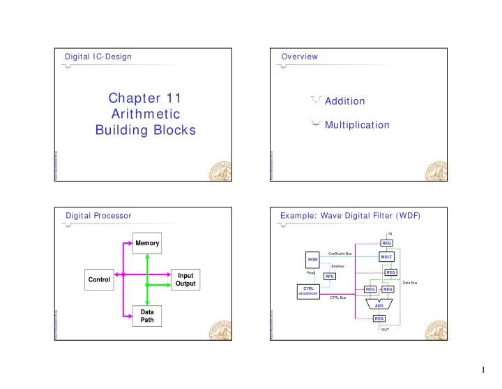
Digital IC-Design Overview Chapter 11 h Addition Arithmetic Multiplication Building Blocks g Digital Processor Example: Wave Digital Filter (WDF) IN Memory REG Coefficient Bus MULT ROM Address REG Read Input APU Control
Digital IC-Design Overview Chapter 11 h Addition Arithmetic Multiplication Building Blocks g Digital Processor Example: Wave Digital Filter (WDF) IN Memory REG Coefficient Bus MULT ROM Address REG Read Input APU Control Output Data Bus CTRL REG NEG SEQUENCER CTRL Bus ADD Data Path REG OUT 1
Data Path Design Bit-Sliced Data Path IN Register Bit Bit 5 Bit Bit 4 Bit Bit 3 Bit Bit 2 Bit 1 Bit Bit 0 Bit Bit-sliced Register XOR design XOR Adder CTRL Adder One slice Register Register per bit Register Register OUT Number Representation Two’s complement conversion Sign Magnitude One´s Complem. Two´s Complem. Invert the number Two´s Complem. Dec. Dec Pos Pos. Neg. Neg Dec. Dec Pos Pos. Neg Neg. Dec Dec. Pos Pos. Neg. Neg Add 1 Add 1 on LSB position LSB iti 0 0000 1000 0 0000 1111 0 0000 Dec. Pos. Neg. 1 0001 1001 1 0001 1110 1 0001 1111 0 0000 2 0010 1010 2 0010 1101 2 0010 1110 Example: 1 0001 1111 3 0011 1011 3 0011 1100 3 0011 1101 2 0010 1110 4 0100 1100 4 0100 1011 4 0100 1100 3 0011 1101 5 0101 1101 5 0101 1010 5 0101 1011 0 1 1 0 6 4 0100 1100 6 0110 1110 6 0110 1001 6 0110 1010 7 7 0111 0111 1111 1111 7 7 0111 0111 1000 1000 7 7 0111 0111 1001 1001 5 5 0101 0101 1011 1011 1 0 0 1 6 8 1000 6 0110 1010 1 7 0111 1001 Two Zeros Two Zeros One Zero 1 0 1 0 -6 8 1000 One more neg. 2
Binary Adder Cell (Two’s Complement) Addition A B B C i S C o A Addition is the most common arithmetic HA C o 0 0 0 0 0 0 0 0 0 Delete 0 Delete operation in digital processors ti i di it l 0 0 1 1 0 Delete S 0 1 0 1 0 Propagate A B Also the basis of most other arithmetic 0 1 1 0 1 Propagate operations like C i FA C o 1 0 0 1 0 Propagate multiplication S division division 1 1 0 0 1 1 0 0 1 Propagate 1 Propagate A B square root 1 1 0 0 1 Generate … C i C o 1 1 1 1 1 Generate S Binary Adder Generate, Propagate, and Delete Half Adder A B = Delete, D A B = ⊕ Functions S A B HA C o = ⊕ ⊕ Propagate Propagate, P P A A B B of A and B = C AB S o = Generate, A B A+ B G AB A B 0 0 0 0 1 1 Full adder C i FA C o 1 0 1 = ⊕ ⊕ = ⊕ = ⊕ ⊕ = S A B C P C S A B C 1 1 1 S = + + = + + = A B = + + + C AB AC BC AB ( A B C ) ABC ABC ABC ABC o C i C o = + + = + + ⊕ = + C AB AC BC AB ( AB A B C ) G PC o S Redundant 3
Ripple Carry Adder Static CMOS Full Adder B 0 A 0 B 1 A 1 B 2 A 2 B 3 A 3 B 4 A 4 V DD C B A V DD B B A A A A FA FA FA FA FA FA FA FA FA FA C C i,0 C o,0 C o,1 C o,2 C o,3 C o,4 B B V DD C Critical A C o C S path S S 0 S 1 S 2 S 3 S 4 C A C Worst case delay A B B A B C B = − + + A A t t ( ( N N 1) 1) t t t t adder carry sum V DD = Ο i e . . t ( N ) C o adder Fast carry more important than fast sum Static CMOS Full Adder - Mirror Adder The Mirror Adder The NMOS and PMOS chains are completely symmetrical One stage operation (inverse) Focus on carry stage Focus on carry stage P P D D V DD A V DD V DD Max two stacked transistors in the carry generation A B B A B C B C A C o C S Transistors connected to C i are placed closest to the output C A C Transistors in the carry stage have to be optimized for speed A B B A B C B A Transistors in the sum stage can be minimal size G P In layout, focus on capacitance at node C o Minimum sized transistors in sum 4
One Stage Addition Digital IC-Design Eliminate carry inversion B A B A Chapter 11 Arithmetic h C i FA FA C i C o C o Building Blocks S S De Morgan Law´ s = S A B C ( , , ) S A B C ( , , ) Cont. = C A B C ( , , ) C A B C ( , , ) One Stage Addition Improved Carry Stage V DD V DD A B B A B B Even Odd A A C 0 C o,0 C 1 C o,1 Few transistors in Few transistors in C i,1 B 0 A 0 B 1 A 1 B 2 A 2 B 3 A 3 B 4 A 4 carry stage A A A B B A B B C i,0 FA FA FA FA FA C o,0 C o,1 C o,2 C o,3 C o,4 P and G precalculated S 0 S 1 S 2 S 3 S 4 V DD V DD before carry before carry G P P G arrives Two different cells C o,0 C o,1 C i,1 P G G P 5
Carry Chain Example – Generate, A = 1 and B = 1 No inversion of A and B needed = + + = + ⊕ = + C AB ( A B ) C AB ( A B ) C G P C o = + + = + ⊕ = + C AB ( A B ) C AB ( A B ) C G P C o V DD V DD V DD V DD 1 1 0 0 G P P G G P P G 0 C o,0 C o,1 C o,0 C o,1 C i,1 C i,1 1 0 0 P G G P 1 P 1 G G P 1 1 A A A A P P P 1 P 0 1 0 G G G G 1 1 B B B B Example – Generate, A = 0 and B = 0 Example – Propagate, A and B Unequal = + + = + ⊕ = + = + + = + ⊕ = + C AB ( A B ) C AB ( A B ) C G P C C AB ( A B ) C AB ( A B ) C G P C o o V DD V DD V DD V DD 0 0 0 1 0 1 G P P G G P P G C o,0 C o,1 C o,0 C o,1 C i,1 C i,1 1 C i,1 C i,1 1 0 0 P 0 G G P 1 P 0 G G P 0 0 0 0 A A A A 0 1 1 0 P P P P G 0 G 1 G 0 G 1 0 0 1 1 B B B B 6
Adder using “ P and G ” XOR in Transmission Gate Full Adder = Delete, D A B = ⊕ Propagate, P A B Even = Generate, G AB B B A A B B = ⊕ P A B Odd B Transmission Gate XOR Transmission Gate Full Adder np-CMOS Adder A B C P S C V DD V DD B O N-Block φ φ P B 0 0 0 0 1 1 C V DD A B C A Single stage φ A 0 0 1 0 0 1 A S S C C i,1 C C B B operation A C 0 1 0 1 0 1 C A B B S 0 φ B B 0 1 1 1 1 0 φ φ Very low load P-Block C o,0 B in critical path 1 0 0 1 0 1 C A A O 1 0 1 1 1 0 C V DD V DD i.e. Very fast B P φ φ V DD N-Block 1 1 0 0 1 0 φ φ B B A B B S 0 1 1 1 0 0 0 C 17 Trans. A C i,0 C B φ A B C A Only 16 transistors! φ φ P-Block C o,1 (24 if we count the inversion of B , S , and C O ) 7
NORA Carry Bypass B C i S C o A 0 0 0 0 0 Delete 0 0 1 1 0 Delete Only Carry Path Shown B A 0 1 0 1 0 Propagate 0 1 1 0 1 Propagate V DD V DD φ φ 1 1 0 0 0 0 1 1 0 Propagate 0 P t FA C i 1 0 1 0 1 Propagate V DD A B B φ C o φ C o,1 φ 1 1 0 0 1 Generate A C o,0 C i,0 A 1 1 1 1 1 Generate φ φ φ S A B B ≠ = φ φ give A B C C o i = A B give C independent of C o i = ⊕ Propagate, Inverting elements between registers!!! P A B Bypass carry if P=1 Carry Bypass Carry Bypass Adder P 0 P 1 P 2 P 3 B 0 A 0 B 1 A 1 P 0 P 1 P 0 G 0 P 1 G 1 P 2 G 2 P 3 G 3 0 0 1 1 2 2 3 3 FA FA C i,0 C o,0 C o,1 C 0 C 1 C 2 C 3 FA FA FA FA C o3 S 0 S 1 S 2 S 3 = ≠ ≠ C C if A B and A B o ,1 i ,0 0 0 1 1 = Bypass if P 0 P 1 P 2 P 3 = 1 that is C C if P P o ,1 i ,0 0 1 otherwise independent of C C Otherwise C o3 independent of C 0 o ,1 i ,0 Bypass carry when P 0 P 1 8
Carry Bypass Adder Carry Ripple v.s. Carry Bypass If A = B in at least one adder cell ⇒ t adder C o not dependent on C i Setup Setup Setup Setup FA FA FA FA FA FA FA FA FA FA FA FA FA FA FA FA S 0 S 1 S 2 S 3 S 4 S 5 S 6 S 7 S 8 S 9 S 10 S 11 S 12 S 13 S 14 S 15 N = 4-8 If A ≠ B in all adders ⇒ Bypass Carry N Carry Select Carry Select: Critical Path Setup Setup Setup Setup Setup "0" 0 0 0 0 0 0 0 0 FA FA FA FA FA FA FA FA FA FA FA FA FA FA FA FA FA FA FA FA 1 1 1 1 FA FA FA FA FA FA FA FA FA FA FA FA FA FA FA FA "1" FA FA FA FA C o,3 C o,7 C o,11 C i,0 C C i,k C C o,k+3 Sum Gen. Sum Gen. Sum Gen. Sum Gen. S 0 S 1 S 2 S 3 S 4 S 5 S 6 S 7 S 8 S 9 S 10 S 11 S 12 S 13 S 14 S 15 Sum Gen. Large area (two adders not needed in first stage) S 0 S 1 S 2 S 3 9
Linear Carry Select Square Root Carry Select Setup Setup Setup Setup Setup Setup Setup Setup 0 0 0 0 0 0 0 0 FA FA FA FA FA FA FA FA FA FA FA FA FA FA FA FA FA FA FA FA FA FA FA FA FA FA FA FA FA FA FA FA 0 0 0 0 0 0 0 0 FA FA FA FA FA FA FA FA FA FA FA FA FA FA 1 FA FA FA FA 1 FA FA FA FA 1 FA FA FA FA 1 FA FA FA FA 1 1 1 1 FA FA FA FA FA FA FA FA FA FA FA FA FA FA C o,3 C o,7 C o,11 C o,1 C o,4 C o,8 C i,0 C i,0 Sum Gen. Sum Gen. Sum Gen. Sum Gen. Sum Sum Sum Gen. Sum Gen. S 0 S 1 S 2 S 3 S 4 S 5 S 6 S 7 S 8 S 9 S 10 S 11 S 12 S 13 S 14 S 15 S 0 S 1 S 2 S 3 S 4 S 5 S 6 S 7 S 8 S 9 S 10 S 11 S 12 S 13 The same number of bits in each stage Adder Delays - Comparison Carry Look Ahead (CLA) t adder = + + = + c ab c (a ( b) ) G c P Ripple o o i i i i = + c G c P o,0 0 i,0 0 Linear = + = + + c G c P G G P c P P o,1 1 o,0 1 1 0 1 i,0 0 1 = + = + + + Square Root Square Root c G G c P P G G G G P P G G P P P P c P P P P P P o,2 2 o,1 2 2 1 2 0 1 2 i,0 0 1 2 N 10
Recommend
More recommend
Explore More Topics
Stay informed with curated content and fresh updates.
