Chapter 1: The digital abstraction Computer Structure - Spring 2004 - PDF document
Chapter 1: The digital abstraction Computer Structure - Spring 2004 Dr. Guy Even c Tel-Aviv Univ. p.1 Digital Circuits vs. Analog Devices Property Digital Circuit Analog Device values { 0 , 1 } description simple (Boolean
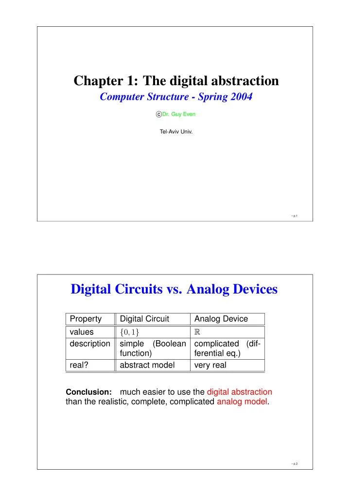
� Chapter 1: The digital abstraction Computer Structure - Spring 2004 � Dr. Guy Even c Tel-Aviv Univ. – p.1 Digital Circuits vs. Analog Devices Property Digital Circuit Analog Device values { 0 , 1 } description simple (Boolean complicated (dif- function) ferential eq.) real? abstract model very real Conclusion: much easier to use the digital abstraction than the realistic, complete, complicated analog model. – p.2
Preliminary questions what is an analog device? (components, behavior) in what way does a digital circuit model an analog device? can every analog device be modeled as a digital circuit? what type of digital circuits do we want? why is one inverter better than another? how can we tell if an analog device is a gate (say, an inverter)? – p.3 Transistors Computers ⇐ VLSI chips ⇐ gates & flip-flops ⇐ transistors Transistors are the basic components. Most common VLSI technology is called CMOS. In CMOS: only two types of transistors: N-transistor P-transistor in case you are curious: VLSI = Very Large Scale Integration (which means “millions of transistors placed on one small chip”) CMOS = Complementary Metal Oxide Semiconductor (which means that both NMOS and PMOS transistors are used). – p.4
N-transistor & P-transistor drain source gate gate source drain N−transistor P−transistor Inputs: gate & source Output: drain (not accurate! just for the sake of this discussion) – p.5 N-transistor & P-transistor drain source gate gate source drain N−transistor P−transistor Functionality of N-transistor: If v ( gate ) = high , then resistance ( source, drain ) = 0 (and then v ( drain ) ← v ( source ) ) If v ( gate ) = low , then resistance ( source, drain ) = ∞ Functionality of P-transistor: If v ( gate ) = high , then resistance ( source, drain ) = ∞ If v ( gate ) = low , then resistance ( source, drain ) = 0 Story true if: v ( s ) = high in P & v ( s ) = low in N. – p.6
Example: a CMOS inverter 5 volts P−transistor IN OUT N−transistor 0 volts IN = low : P-transistor is conducting N-transistor is not conducting ⇒ v ( OUT ) = high IN = high : P-transistor is not conducting N-transistor is conducting ⇒ v ( OUT ) = low – p.7 Qualitative Analysis vs. Quantitative Analysis Qualitative analysis: gives an idea about “how an inverter works”. no idea about actual voltages of output as a function input voltage. no idea about how long it takes the output to stabilize. Quantitative analysis: based on precise modeling of transistor. computes precise input-output relationship. requires a lot of work (usually done with the aid of a computer program called SPICE). – p.8
� � � Analog signals An analog signal is a real function f : → , where f ( t ) = voltage as a function of the time. Assumption: wires have zero resistance, zero capacity, and signals propagate through wires without delay. ⇒ voltage along a wire is identical at all times. Since a signal describes the voltage (i.e. derivative of energy as a function of charge), we also assume that a signal is a continuous function. – p.9 Digital signals A digital signal is a function g : → { 0 , 1 , non-logical } . The value of a digital signal describes the logical value carried along a wire as a function of time. zero & one : logical values. non-logical: indicates that the signal is neither zero or one. – p.10
Interpreting analog signals as digital signals Q: How does one interpret an analog signal as a digital signal? naive answer: define a threshold voltage V ′ . Consider an analog signal f ( t ) . The digital signal dig ( f ( t )) is defined as follows. � if f ( t ) < V ′ 0 △ dig ( f ( t )) = 1 if f ( t ) > V ′ Q: is this a useful definition? – p.11 problems with definition of dig ( f ( t )) All devices in a circuit must use exactly the same threshold V ′ . This is impossible due to manufacturing tolerances. Perturbations of f ( t ) around V ′ lead to unexpected values of dig ( f ( t )) . Example: Measure weight w by measuring the length ℓ of a spring. Suppose we wish to know if w > w ′ . This can be done by checking if ℓ > ℓ ′ . However, spring length oscillates around ℓ . If ℓ ≈ ℓ ′ , then comparison requires a long time. ⇒ must use separate thresholds for 0 and for 1 . – p.12
Interpreting analog signals as digital signals Q: How does one interpret an analog signal as a digital signal? A: Two voltage thresholds are defined: V low < V high . Consider an analog signal f ( t ) . The digital signal dig ( f ( t )) is defined as follows. 0 if f ( t ) < V low △ 1 if f ( t ) > V high dig ( f ( t )) = non-logical otherwise. – p.13 digital interpretation of an analog signal f ( t ) logical one V high V low logical zero t – p.14
did we solve the problems of a single threshold? manufacturing requirements: a low output must be ≤ V low & a high output must be ≥ V high . fluctuations of f ( t ) around V low still cause fluctuations of dig ( f ( t )) . However, these fluctuations are between 0 and “non-logical” (not between 0 and 1 ). This is still a problem, but not as bad... Will noise cause a problem? Noise = undesired changes to f ( t ) . Back to the example of a weight hanging from a spring: wind causes changes in the spring length and disturbs measurement of spring length. – p.15 An inverter Q: define an inverter. A: 0 if dig ( IN ( t )) = 1 △ dig ( OUT ( t )) = 1 if dig ( IN ( t )) = 0 arbitrary otherwise. We will see shortly that: noise ⇒ cannot use these definitions to build correct circuits. Before we can answer that we need to discuss transfer func- tions... – p.16
� � Transfer functions DEF: transfer function - the relation between the voltage at an output of a gate and the voltages of the inputs of the gate. Example: An inverter with an input x and an output y . The value of the signal y ( t ′ ) at time t ′ is a function of the signal x ( t ) in the interval ( −∞ , t ′ ] . Static transfer function: if the input x ( t ) is stable for a sufficiently long period of time and equals x 0 , then the output y ( t ) stabilizes on a value y 0 that is a function of x 0 . history vs. present: if a device does not have a static transfer function, then the device is a memory device not a logical gate. – p.17 Static transfer function Let G denote a gate with one input x and one output y . DEF: A function f : → is a static transfer function of a gate G if ∃ ∆ > 0 ∀ x 0 ∀ t 0 : ∀ t ∈ [ t 0 − ∆ , t 0 ] x ( t ) = x 0 = ⇒ y ( t 0 ) = f ( x 0 ) . ∆ - propagation delay (time required for stable output) x 0 - stable input voltage t 0 - time in which y ( t ) is measured – p.18
Static transfer function - remarks (1) Since circuits operate over a bounded range of volt- ages, static transfer functions are usually only defined over bounded domains and ranges (say [0 , 5] volts). – p.19 Static transfer function - remarks (2) Allow perturbations of x ( t ) and y ( t ) . ∀ ǫ ∃ δ, ∆ > 0 ∀ x 0 , t 1 , t 2 : ∀ t ∈ [ t 1 , t 2 ] : | x ( t ) − x 0 | ≤ δ = ⇒ ∀ t ∈ [ t 1 + ∆ , t 2 ] : | y ( t ) − f ( x 0 ) | ≤ ǫ. δ - measures stability of input x ( t ) ǫ - measures stability of output y ( t ) [ t 1 , t 2 ] - interval during which x ( t ) is δ -stable. [ t 1 + ∆ , t 2 ] - interval during which y ( t ) is ǫ -stable. Propagation delay ∆ depends only on ǫ (which is fixed and the same for all voltages). – p.20
back to the definition of an inverter if dig ( IN ( t )) = 1 0 △ dig ( OUT ( t )) = 1 if dig ( IN ( t )) = 0 arbitrary otherwise. or equivalently, IN ( t ) < V low = ⇒ OUT ( t ) > V high IN ( t ) > V high = ⇒ OUT ( t ) < V low Q: Define a NAND -gate. – p.21 Noise wire A(t) B(t) Noise signal: the difference B ( t ) − A ( t ) . (reference signal = A ( t ) ). Q: what causes noise? A: The main source of noise is heat. Heat causes ran- dom movement of electrons. These random movements do not cancel out perfectly, and random currents are created. These random currents create perturbations in the voltage of a wire. – p.22
Bounded noise model Bounded noise model - the noise signal along every wire has a bounded absolute value. Uniform bounded noise model: ∃ ǫ > 0 such that : | noise | ≤ ǫ. Justification - noise is a random variable whose distribution has a rapidly diminishing tail. If the ǫ is sufficiently large, then Prob [ | noise | > ǫ ] ≈ 0 . – p.23 The digital abstraction in the presence of noise y z x Assume that: x > V high , so dig ( x ) = 1 , y = V low − ǫ ′ , for a very small ǫ ′ > 0 . ⇒ dig ( z ) = 1 . What if input to 2nd inverter equals y ( t ) + n y ( t ) ? If n y ( t ) > ǫ ′ , then dig ( y ) = non-logical, and can’t deduce that dig ( z ) = 1 . ⇒ must strengthen the digital abstraction! – p.24
Recommend
More recommend
Explore More Topics
Stay informed with curated content and fresh updates.


