Automatic Cell Layout in the 7nm Era Pascal Cremer , Stefan Hougardy, - PowerPoint PPT Presentation
Automatic Cell Layout in the 7nm Era Pascal Cremer , Stefan Hougardy, Jan Schneider, and Jannik Silvanus Research Institute for Discrete Mathematics University of Bonn March 21, 2017 1 / 24 Increasing complexity in 7nm cell design SADP / SAQP
Automatic Cell Layout in the 7nm Era Pascal Cremer , Stefan Hougardy, Jan Schneider, and Jannik Silvanus Research Institute for Discrete Mathematics University of Bonn March 21, 2017 1 / 24
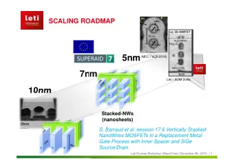
Increasing complexity in 7nm cell design SADP / SAQP LELELELE unroutable placements Manual cell layout becomes much harder 2 / 24
BonnCell fully automatically builds 7nm physical cell layouts optimally DRC-clean DFM-aware Use cases: Interactive prototyping Early stage timing analysis Highly optimized end stage design 3 / 24
1 Placement Branch and bound algorithm check routability minimize area 4 / 24
1 2 Placement Routing Branch and bound algorithm MIP routing check routability LVS + DRC clean routing minimize area respect DFM constraints 4 / 24
Placement Problem Definition Given: D S D Fets D S G G Output: for each fet G number of fingers swap status (swapped or not) position S D S D S G G G 5 / 24
Placement Problem Definition Given: D S D Fets D S G G Output: for each fet G number of fingers swap status (swapped or not) position Target: S D guarantee routability S D S minimize cell width G G G optimize netlength, timing, ... 5 / 24
Fet1 ... ... ... ... Fet3 ... ... ... Fet2 ... ... 1 fjnger ... ... Fet3 Fet2 unswapped swapped 2 fjngers x = 0 x = 1 x = 2 6 / 24
Fet1 1 fjnger ... ... ... Fet3 ... ... ... Fet2 ... ... ... ... ... Fet3 Fet2 unswapped swapped 2 fjngers x = 0 x = 1 x = 2 Number of nodes 9 . 2 × 10 14 → 7 . 8 × 10 6 (9 fets, 15 tracks) 6 / 24
Design Rules Two fets can share contacts if heights are equal neighboring TS nets are equal otherwise they need a gap in between 7 / 24
Design Rules Two fets can share contacts if heights are equal neighboring TS nets are equal otherwise they need a gap in between A B A A B A 7 / 24
Design Rules Two fets can share contacts if heights are equal neighboring TS nets are equal otherwise they need a gap in between A B A A B A B A B A B A 7 / 24
Design Rules Two fets can share contacts if heights are equal neighboring TS nets are equal otherwise they need a gap in between A B A A B A B A B A B A B A A B A 7 / 24
Graph Formulation A B B C C E C A E G C D K B F H Determine lower bound on placement width by solving Minimum Vertex Cover Partition into s - t -walks 8 / 24
Further Design Rules / Constraints PC cut shapes Routability Mx cut shapes 9 / 24
CT Algorithm 1: for x 1 , y 1 ∈ B ⋆ ∩ [ l 1 , u 1 ] with y 1 − x 1 ≥ d do Set [ x 1 , y 1 ] as solution of P 1 ( x 1 , y 1 ) 2: 3: end for 4: for i = 2 , . . . , n do for x i , y i ∈ B ⋆ ∩ [ l i , u i ] with y i − x i ≥ d do 5: for [ x i − 1 , y i − 1 ] s.t. P i − 1 ( x i − 1 , y i − 1 ) has a solution and 6: [ x i − 1 , y i − 1 ] , [ x i , y i ] are legal neighbors do Set [ x i − 1 , y i − 1 ] , [ x i , y i ] as solution of P i ( x i , y i ) 7: end for 8: end for 9: 10: end for 11: Pick legal cut shape on track n and use backtracking to obtain entire solution. Theorem The CT Algorithm solves the PC cut shapes problem in O ( n 5 ) time, for the number of PC tracks n . In practice it has running time O ( n ). 10 / 24
Routing During Placement Three modes from a broad spectrum PC Cut Full Routing Pin Access Shapes fast fastest most expensive excludes many guarantees legal guarantees unroutable PC cut shapes routability placements 11 / 24
Routing During Placement: Pin Access Mode 12 / 24
Routing During Placement: Solution Expected by Designer 13 / 24
Routing During Placement: Full Routing Mode 14 / 24
Routing – Features Grid-based Fully flexible metal Flexible via positions connectivity cut shape positions 15 / 24
Routing – MIP Formulation – Connectivity MIP - modeled as Steiner tree packing problem in graphs State of the art formulations are key to fast running times Unidirected cut relaxation (Integrality gap 2) Bidirected cut relaxation (Worst known example has integrality gap 8 / 7) Multicommodity flow relaxation � min c e x e e ∈ E = � x k s.t. x e ∀ e ∈ E e k ∈N ∈ { 0 , 1 } ∀ e ∈ E x e x k ∈ { 0 , 1 } ∀ e ∈ E , k ∈ N e � 1 if i = r k f t ( v ) = − 1 if i = t 0 else ∀ v ∈ V , k ∈ N , t ∈ S k ≤ f t x k 0 ≤ � ∀ ( i , j ) ∈ A , k ∈ N , t ∈ S k ij ij x k x k ≤ x k � ij + � ∀ { i , j } ∈ E , k ∈ N ji { i , j } 16 / 24
Routing – Design Rules Exact representation of all Design Rules (DRC + DFM) Cut shapes – cut shape spacing Via metal overhangs Metal min area Via coloring Via – via spacing with flexible via positions Many more ... Full Optimization of netlength 17 / 24
18 / 24
19 / 24
20 / 24
21 / 24
22 / 24
Standard logic Latches 2 – 14 fets 28 – 36 fets 5 – 16 nets 21 – 28 nets 4 – 12 CPP 22 – 32 CPP 14nm comparison: highly complex BonnCell improves area for 43% of used many times on chip all library cells Manual layout work: weeks 23 / 24
Standard logic Latches 2 – 14 fets 28 – 36 fets 5 – 16 nets 21 – 28 nets 4 – 12 CPP 22 – 32 CPP 14nm comparison: highly complex BonnCell improves area for 43% of used many times on chip all library cells Manual layout work: weeks BonnCell Minimal area Placement LVS, DRC, and DFM clean Routing Standard logic ≤ 6min Latches ≤ 19h 23 / 24
BonnCell fully automatically builds 7nm physical cell layouts optimally DRC-clean DFM-aware Use cases: Interactive prototyping Early stage timing analysis Highly optimized end stage design Thank you! 24 / 24
Recommend
More recommend
Explore More Topics
Stay informed with curated content and fresh updates.
