500C Electronic Packaging and Dielectric Materials for High - PowerPoint PPT Presentation
https://ntrs.nasa.gov/search.jsp?R=20170003040 2018-04-09T08:08:43+00:00Z National Aeronautics and Space Administration NAECON OIS 9:30AM July 29, 2016 500C Electronic Packaging and Dielectric Materials for High Temperature Applications
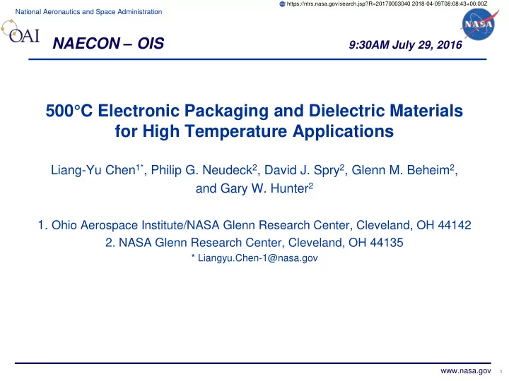
https://ntrs.nasa.gov/search.jsp?R=20170003040 2018-04-09T08:08:43+00:00Z National Aeronautics and Space Administration NAECON – OIS 9:30AM July 29, 2016 500°C Electronic Packaging and Dielectric Materials for High Temperature Applications Liang-Yu Chen 1* , Philip G. Neudeck 2 , David J. Spry 2 , Glenn M. Beheim 2 , and Gary W. Hunter 2 1. Ohio Aerospace Institute/NASA Glenn Research Center, Cleveland, OH 44142 2. NASA Glenn Research Center, Cleveland, OH 44135 * Liangyu.Chen-1@nasa.gov www.nasa.gov 1
National Aeronautics and Space Administration Presenter • Liang-Yu Chen • Senior Scientist • Ohio Aerospace Institute (OAI) / NASA Glenn Research Center • Ph.D. in experimental solid state physics/Case Western Reserve University • Research Interests – Packaging materials, process, design, and testing for high temperature SiC electronics and sensors for aerospace applications • Currently supporting high temperature electronics/sensor packaging research at NASA Glenn Research Center www.nasa.gov 2
National Aeronautics and Space Administration 500°C Electronic Packaging and Dielectric Materials for High Temperature Applications 9 :30 AM July 29, 2016 Outline Background • SiC and SOI electronics and sensors, aerospace applications • Packaging/integration concepts/functions • Conventional electronics packaging material system issues High temperature ceramic packaging systems • Dielectric properties of selected alumina and aluminum nitride • Metallization for high temperature applications • Prototypes of packages and PCBs • Results of laboratory tests, space and flight test with SiC electronics • SOI circuits for Distributed Engine Control • Circuit level test above commercial temperature limit • Specifications vs T and derating? Sensor packaging – capacitive pressure sensor Dielectric for high temperature capacitors Summary Acknowledgements www.nasa.gov 3
National Aeronautics and Space Administration Background: High Temperature Devices and Packaging Background 500°C SiC electronics and MEMS sensors have been demonstrated • JFET ICs, MEMS based pressure sensor and Schottky diode based gas chemical sensors • Applications include aerospace engine control and long term Venus probes Commercial SOI ICs for 225°C, operable at T > 225°C for Distributed Engine Control ? Conventional packaging technologies • Plastic materials melt, de-polymerize, and burn at high temperatures • Conductor and alloys (solder) melt and oxidize rapidly at high temperatures • High thermal stress due to thermal expansion mismatch - mechanical failure at structure level • Challenges at material and structure levels www.nasa.gov 4
National Aeronautics and Space Administration Background: Packaging Concepts Packaging Technology for Electronics/Sensors Packaging is essential to microelectronics and sensors – Mechanical support – Electrical interconnection – Electromagnetic, chemical environment Chip-level packaging – Substrate and metallization – Die-attach – Wire-bonding Printed Circuit Board (PCB) – Interconnecting packaged chips and passives PCB edge connectors − Subsystem level packaging Capacitive pressure sensor packaging – Spark-plug type – High differential pressure environment www.nasa.gov 5
National Aeronautics and Space Administration Background: Temperature Dependent Dielectric Properties of Polycrystalline Al 2 O 3 Substrates Dissipation Factor of selected 96% Al 2 O 3 Dissipation Factor of selected 92% Al 2 O 3 substrate at various frequencies substrate at various frequencies • Dissipation factors changes with T and f significantly • Dissipation factor is purity/impurity dependent • Dissipation factor of selected 96% is lower compared with selected 92% www.nasa.gov 6
National Aeronautics and Space Administration Ceramic Packaging Systems for 500°C SiC Electronics Ceramic Chip-level Packages and PCBs 96% Al 2 O 3 90% Al 2 O 3 AlN • Three types of ceramics and Au thick-film metallization based chip- level packages and printed circuit boards (PCBs) • Chip-level packages characterized between room temperature and 500 o C • Tested with SiC ICs at 500 o C and thermal cycled www.nasa.gov 7
National Aeronautics and Space Administration Packaging Systems for 500 ° C SiC Electronics - 96% alumina packaging system - laboratory test 96% Alumina Chip-level Packages I/O1 –“Ground” I/O2 I/O3 (a) Parasitic Equivalent (b) I/O i I/O j 0.5 inches (c) (d) Parasitic Capacitance and Conductance of Neighboring I/Os T ( o C) T R 100 150 200 250 300 350 400 450 500 550 f (Hz) Usable for 0.00nF 0.00nF 5 0.00nf 0.00nF 0.00nF 0.00nF 0.00nF 0.00nF 0.00nF < 5 100 0.00 0.00 0.00 0.00 0.00 0.00 0.00 0.00 0.00 0.005 0.00 packaging many 0.5 0.5 0.5 1 1 1 1.5 1.5 1.5 1.5 2 120 envisioned low 0.000 0.000 0.000 0.000 0.000 0.000 0.000 0.000 0.0005 0.001 0.001 0.5 0.5 0.95 0.5 0.5 0.5 0.5 0.6 0.7 0.7 0.8 power 500 ° C 1K 0.000 0.000 0.000 0.000 0.000 0.000 0.000 0.001 0.001 0.002 0.0025 devices/ circuits 0.49 0.50 0.50 0.490 0.49 0.52 0.53 0.58 0.59 0.65 0.69 10K 0.001 0.000 0.008 0.000 0.000 0.000 0.001 0.002 0.003 0.004 0.006 0.492 0.486 0.497 0.493 0.487 0.517 0.539 0.535 0.563 0.585 0.57 100K pF 0.005 0.0015 0.022 0.030 0.006 0.002 0.003 0.005 0.007 0.011 0.015 μ S 0.501 0.497 0.485 0.506 0.499 0.529 0.533 0.55 0.556 0.544 0.55 1M - - - - - - - - - - - www.nasa.gov 8
National Aeronautics and Space Administration Packaging Systems for 500 ° C SiC Electronics - 96% alumina packaging system - laboratory test Test Results of Packaged SiC JFET 1 cm Al 2 O 3 Al 2 O 3 Differential 200μm/10μm Amplifier 6H-SiC JFET • A packaged SiC JFET characterized at 500 o C • Less than 7% change in the JFET characteristics in first 6000 hours • Tested at 500 o C for over 10,000 hrs • Demonstrated for long term operation at 500 o C for the first time www.nasa.gov 9
National Aeronautics and Space Administration Packaging Systems for 500 ° C SiC Electronics - 96% alumina packaging system – space and flight test Space and Flight Test of 96% Alumina Packaging System 96% Al 2 O 3 90% Al 2 O 3 • 96% alumina chip-level packaging, PCB, and joining materials • First flight and space test of 96% alumina high temperature harsh environment packaging system • Monitor packaged SiC JFET DC parameter and compare with a SiC JFET in a conventional package www.nasa.gov 10
National Aeronautics and Space Administration Packaging Systems for 500 ° C SiC Electronics - 96% alumina packaging system – space and flight test Space and Flight Test of 96% Alumina Packaging System 96% Al 2 O 3 90% Al 2 O 3 • MISSE7 suite exposed to Shuttle launch, atomic oxygen, space radiation, thermal cycling, and reentry • In an aluminum box • Eighteen months on ISS orbit www.nasa.gov 11
National Aeronautics and Space Administration Packaging Systems for 500 ° C SiC Electronics - 96% alumina packaging system – space and flight test On-orbit I-V Data of Packaged SiC JFETs TO-8 40µm/10µm JFET T = 296 K 40µm/10µm HT-JFET T = 296 K 0.8 0.8 V V 0 hours 0 h G G D (mA) 4304 h D (mA) 4304 hours 0V 0V 0.6 0.6 -1V -1V Drain Currnet I Drain Currnet I -2V 0.4 -2V 0.4 -3V -4V -4V 0.2 0.2 -6V -5V -6V -8V 0.0 -10V -8V 0.0 0 5 10 15 0 5 10 15 Drain Voltage V D (V) Drain Voltage V D (V) • I-V data acquired every hour with temperature measurement • Eighteen months on orbit • Latest set of V DS vs. I D curves shows no degradation • No packaging degradation/failure detected after space and flight tests www.nasa.gov 12
National Aeronautics and Space Administration Co-fired Alumina High Temperature Packaging System Co-fired Alumina • 96% alumina substrate based packaging system – Dielectric properties of 96% alumina measured at temperatures up to 550 C – Excellent electrical and dielectric properties as substrate for conventional electronics – Thin-film and thick-film metallization available – 96% alumina packaging system long term tested with SiC electronics at 500 o C – Chip-level packages not fabricated with co-fired process • Low temperature and high temperature co-fired (LTCC and HTCC) alumina substrates ? − A few percent of glass used in co-fired alumina systems − Suitable for large scale commercialization − Dielectric performance at high temperatures? − Co-fired metallization www.nasa.gov 13
National Aeronautics and Space Administration Co-fired Alumina High Temperature Packaging System Dielectric Constant AC Conductivity 300 C, Dielectric constant of selected HTCC alumina stable below increases slightly with T above 300 C – less compared with 96% alumina and selected LTCC alumina AC conductivity of selected HTCC alumina is lower and increases less compared with selected 96% alumina and LTCC alumina www.nasa.gov 14
Recommend
More recommend
Explore More Topics
Stay informed with curated content and fresh updates.
