1 whatever is the poorest, is going to be limiting overall - PDF document
MITOCW | 4. Charge Excitation The following content is provided under a Creative Commons license. Your support will help MIT OpenCourseWare continue to offer high quality educational resources for free. To make a donation or view additional
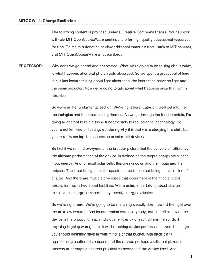
MITOCW | 4. Charge Excitation The following content is provided under a Creative Commons license. Your support will help MIT OpenCourseWare continue to offer high quality educational resources for free. To make a donation or view additional materials from 100's of MIT courses, visit MIT OpenCourseWare at ocw.mit.edu. PROFESSOR: Why don't we go ahead and get started. What we're going to be talking about today, is what happens after that photon gets absorbed. So we spent a great deal of time in our last lecture talking about light absorption, the interaction between light and the semiconductor. Now we're going to talk about what happens once that light is absorbed. So we're in the fundamental section. We're right here. Later on, we'll get into the technologies and the cross cutting themes. As we go through the fundamentals, I'm going to attempt to relate those fundamentals to real solar cell technology. So you're not left kind of floating, wondering why it is that we're studying this stuff, but you're really seeing the connection to solar cell devices. So first if we remind everyone of the broader picture that the conversion efficiency, the ultimate performance of the device, is defined as the output energy versus the input energy. And for most solar cells, this breaks down into the inputs and the outputs. The input being the solar spectrum and the output being the collection of charge. And there are multiple processes that occur here in the middle. Light absorption, we talked about last time. We're going to be talking about charge excitation in charge transport today, mostly charge excitation. So we're right here. We're going to be marching steadily down toward the right over the next few lectures. And let me remind you, everybody, that the efficiency of the device is the product of each individual efficiency of each different step. So if anything is going wrong here, it will be limiting device performance. And the image you should definitely have in your mind is of that bucket, with each plank representing a different component of the device, perhaps a different physical process or perhaps a different physical component of the device itself. And 1
whatever is the poorest, is going to be limiting overall performance. Your efficiency is going to be flowing out from that low plank and you will have a low efficiency device. So the art of making a high efficiency solar cell is really understanding everything that goes into the physical processes, but also the devices. And that's why we break it down like this. We have the physical processes, and finally we get into some of the devices in the architectures of manufacturing methods. So learning objectives today. Oops. That was a little bit of a typo. It's not the solar resource. We're talking about charge excitation today. We will be talking phenomena logically how this thing called a band gap forms. It's a very important physical concept. We'll lead off the lecture with it, and then very quickly go into applications that you see why it's important, returning back to the fundamentals, how it actually forms, going back and forth until we have a pretty solid understanding. From the background surveys, I understand that about 50% of you understand what a band gap is. So 50% of you may be a little bored, or a little entertained, at my hand wave explanations during the first part of class. I encourage you to think about the band gap from the perspective of the solar cell device, because this is probably not something you've done before. You've probably understood band gap from the perspective of a semiconductor device as packaged in the dark, perhaps in a little gadget like this. But not something that's exposed to light with the addition of a generation current. Or at least not in detail. So I welcome you to think about that as we go through the explanations in the beginning of class. Then we'll describe how optical absorption in semiconductors represents the transitions of charge in an energy band diagram. In other words, if we imagine a given space of the semiconductor divisive, say a surrounding of a given atom, and we imagine that different orbitals, different electron orbitals will have different energies associated with them. We are going to be talking about how light gets absorbed in transitions electrons between those different energy orbitals. That's important because then we'll be able to calculate the fraction of photons lost, 2
not absorbed, by a given semiconductor material. We'll be able to calculate the fraction of incident solar energy that is lost as well, due to a phenomenon called thermalization. And finally, we're going to be able to plot efficiency versus band gap, and denote specific materials on it. In other words, we are going to be doing our first higher level efficiency calculations for a solar cell device by the end of today's lecture. And the idea is to expose a little bit on the technology side as well, so that you have an appreciation for what's up and coming in the field, what are some of the ways to enhance the performance of social devices. So band gap. Very, very basic description. If you've never been exposed to band gaps before, the reason it's important is because the band gap is going to define what color, what portion of the solar spectrum that material absorbs light most efficiently. How a band gap forms is related to the atomic structure. Think of bonds as essentially why stuff is tough. If the mechanical engineers in the room, if you remember linear elasticity, those bonds are what are essentially forming those springs between the atoms that are keeping them, the material, from flying apart. There is also a very interesting property here, that if you have a bound electron, it's usually not moving very far that atom. It's usually in a very localized electronic state close to that atom. So if you were to apply a resistance meter, an Ohm meter, to your device to measure the resistance across it, and you had just bound electrons, you would measure a very, very low current passing through that material. Because there would be very few free charge carriers to move in that applied field, when you apply the two probes and there's a little battery in here that applies a field across the material, you wouldn't be able to measure much current flow, because there wouldn't be too many free electrons to carry that current. So the bound electrons essentially enhance the strength of the material. But it doesn't help us from a semiconductor point of view. What we need are excited electrons. And excited electrons are why materials conduct. So let's imagine we 3
have a bond. For example, in this material right here, these gray lines are really two electrons that are covalently bonded. Essentially two electrons-- one electron from each little black circle representing a carbon atom. And each electron associated with that carbon atom is shared with the other, in a covalent bond. And for the chemists in the room, more precisely, you have sp3 hybridized orbitals in this diamond cubic crystal structure. For everyone else, these are shared electrons in a covalent bonding configuration. Now if light comes in with enough energy, it can excite an electron from that covalently bonded state into an excited state, where it can then roam freely throughout the lattice. And that's the nature of charge excitations. So the big question that we have to ask ourselves is, what color of light will this material absorb most effectively? Will those electrons in the covalent bonds absorb light and be excited into a state where they can roam freely around the material, and ultimately conduct electricity? OK. So the answer to that question is not simple. Understanding how a band gap forms can be an entire semester of quantum physics. But what we're going to do is do it in a three step approach. Simple, very, very simple explanations that hopefully everyone will get. The next most simple explanation, which hopefully 80% of you will get, and then perhaps a more detailed explanation that only a few of you will get. But the idea is to really progress in levels of explanation. So let me go back one step. Yeah. The band gap energy can be most simply understood as a finite amount of energy needed to excite a highly localized electron into a de-localized excited state in the semiconductor where it can move around the crystal. OK. So this is the description of the band gap, how a band gap forms that you'll see in many chemistry textbooks. And I like it, because it's something that you can really grasp and understand. We have to start with the simple premise that electrons are a type of particle called a fermion. What is a fermion? Let's refresh our basic physics here. What means a fermion? Spin one half. And it also means-- can two fermions occupy the same state? No, 4
Recommend
More recommend
Explore More Topics
Stay informed with curated content and fresh updates.
